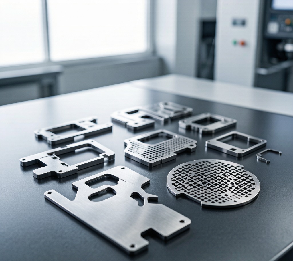
Photochemical etching services solve a problem that laser cutting and stamping both struggle with: making very thin, very intricate metal parts that are completely flat, completely burr-free, and completely free of heat-affected zone. The process uses light and acid instead of tools. A photoresist image of your part is exposed onto sheet metal, developed, and the exposed metal is dissolved away by an etchant spray. There is no cutting force, no heat input, and no hard tooling. A design change costs a new photo tool — a piece of film that can be produced in hours for a few hundred dollars — instead of a new die costing tens of thousands.

How Photochemical Etching Works
The sequence is short and highly repeatable. Sheet metal is cleaned to remove oxides and oils, then laminated on both sides with a UV-sensitive photoresist. A photo tool carrying the part image is registered top and bottom, and the sandwich is exposed to ultraviolet light. Developing washes away the unexposed resist, leaving bare metal exactly where material must be removed.
The panel then passes through an etching machine where heated ferric chloride is sprayed onto both faces under pressure. The etchant dissolves metal isotropically, working inward from both surfaces simultaneously until the two etch fronts meet in the middle. Finally the remaining resist is stripped, parts are separated from their tabs, and the sheet is inspected.
Because etching attacks from both sides, the resulting edge has a characteristic hourglass profile with a slight ridge at mid-thickness. That is normal and is accounted for in the photo tool compensation. Critically, there is no mechanical burr at all — the edges are chemically smooth and need no deburring.
Etching vs Laser Cutting vs Stamping
Laser cutting is faster on thicker material and on simple outlines, and it needs no photo tool at all. But it melts material at the kerf, leaving a recast layer, dross, and a heat-affected zone. On foils under 0.2 mm it also tends to warp the part. Our overview of laser cutting services compares the cut-quality envelope in detail; for anything with hundreds of small apertures in thin stock, etching wins on both cost and quality.
Stamping is unbeatable above roughly 100,000 pieces, but the die is expensive, lead time is weeks, and punching thin material creates a rollover on one face and a burr on the other. It also work-hardens the edge, which matters for springs and contacts. Our guide to precision metal stamping sets out where that crossover sits.
Etching occupies the middle ground and dominates prototype and mid-volume work. Because the photo tool can hold dozens or hundreds of part images on one panel, unit cost falls steeply with quantity while tooling cost stays trivial. That makes it a natural companion to metal rapid prototyping: iterate three design revisions in a fortnight, then scale the winning revision without re-tooling.
Materials and Thickness Limits
Almost any metal that dissolves in an acid etchant can be processed. Stainless steels 301, 304, and 316 are the workhorses. Copper, brass, phosphor bronze, and beryllium copper etch beautifully and are standard for electrical contacts and shielding. Nickel, Invar, Kovar, molybdenum, and titanium are all routinely handled for specialised work. Aluminium can be etched but needs a different chemistry and gives a coarser edge.
Practical thickness runs from 0.01 mm foil to about 2 mm. The sweet spot is 0.05 to 0.8 mm. Above 1.5 mm, etch time and undercut both grow to the point where fiber laser cutting or CNC punching becomes more economical.
The governing design rule is that minimum feature width and minimum hole diameter should be at least 1.0 to 1.2 times the material thickness. On 0.1 mm stainless that means 0.1 mm slots are achievable — a resolution stamping simply cannot reach at that gauge. Web widths between adjacent apertures follow the same rule. Corner radii are naturally formed at roughly half the material thickness.
Tolerances, Finishing and Applications
Standard tolerance is ±10 percent of material thickness with a floor of about ±0.02 mm. On 0.2 mm stock that is ±0.02 mm on feature size, which comfortably satisfies most shim, gasket, and shielding applications. Positional accuracy across a panel is held within ±0.05 mm because the photo tool is dimensionally stable and registration is optical.
Half-etching is a valuable trick: by imaging a feature on one side only, you can produce fold lines, pockets, counterbores, and part-marking recesses at partial depth in the same operation. Bend lines half-etched to 50 percent of thickness let a flat etched part be folded into a three-dimensional shield or clip with no press brake tooling.
Etched parts often go straight to plating or coating. Tin, nickel, and gold plating for contacts, passivation for stainless in medical service, and silk screening for legend and identification are all common downstream steps. Where a flat etched blank must be integrated into a larger fabrication, our sheet metal processing cells handle forming, welding, and assembly.
Typical parts include encoder discs, EMI and RFI shielding cans, lead frames, spring contacts and fingers, fuel cell bipolar plates, filter and sieve meshes, surgical instrument blades, precision shims and washers, heat exchanger fins, and speaker grilles. Anywhere a designer needs hundreds of accurate apertures in thin metal without distortion, etching is the answer, and for larger blanks we combine it with sheet metal laser cutting for the outer profile.
Frequently Asked Questions
How fast can I get etched prototypes? Photo tools are produced the same day from your CAD data, and simple parts in stock material can ship in three to five working days. Complex or plated parts run seven to ten days.
What does the tooling cost? A photo tool typically costs USD 150 to 500 depending on panel size and image complexity, and it is reusable indefinitely. Compare that with USD 8,000 upwards for a comparable stamping die.
Are etched parts really burr-free? Yes. Material is dissolved rather than sheared, so there is no mechanical burr and no rollover. This is the single most common reason customers switch from stamping to etching on thin contact and shim parts.
Does etching change the material properties? No. There is no heat input and no mechanical work, so temper, hardness, magnetic properties, and grain structure are unchanged. Spring materials retain their full temper, which is why beryllium copper contacts are almost always etched.
What is the maximum part size? Panel sizes up to roughly 600 × 900 mm are standard. Individual parts can be as small as 1 mm square or as large as the panel allows.
What files do you need? A DXF or DWG flat pattern is ideal, with separate layers for through features and half-etch features, plus a note specifying material, thickness, temper, finish, and quantity. If you have only a 3D model we will produce the flat pattern and send it for approval before making the photo tool.
Ready to Start Your Project?
Get a build-ready quote on your custom metal parts within 24 hours. Share your drawing and our engineers will respond with process, lead time, and pricing.